

What Is The Memory Buffer Register Size Of The Pentium Processor
Chapter � 2 The Microprocessor & its Compages
�
����������������������������������������������������������������������������������������������������
Introduction
This chapter presents the microprocessor as a programmable device past first looking at its in�ternal programming model so at how information technology addresses its memory space. The addressing modes for Intel family of microprocessors are described for both the real and protected modes of operation. Existent mode memory exists at locations 00000H-FFFFFH the first 1M byte of the memory system�and is nowadays on all versions of the microprocessor. Pro�tected fashion memory exists at any location in the unabridged memory system, just is bachelor but to the 80286�Pentium Two, not to the earlier 8086 or 8088 microprocessors. Protected fashion memory for the 80286 contains 16M bytes; for the 80386-Pentium, 4G bytes; and for the Pentium Pro and Pen�tium Ii, either 4G or 64G bytes.
ii.one. Internal Microprocessor Architecture
Before a plan is written or whatsoever instruction investigated, the internal configuration of the mi�croprocessor must exist known. This section of the chapter details the program-visible internal ar�chitecture of the 8086�80486 and the Pentium�Pentium Two microprocessors. Also detailed are the part and purpose of each of these internal registers.
ii.1.1. The Programming Model
�������� The programming model of the 8086 through the Pentium II�s considered to be program visible because its registers are used during awarding programming and are specified by the instruc�tions. Other registers, detailed later in this affiliate, are considered to be plan invisible exist�cause they are not addressable directly during applications programming, but may be used indirectly during system programming. Simply the 80286 and higher up contain the program-invisible registers used to control and operate the protected retentiveness system.
Effigy ii-1 illustrates the programming model of the 8086 through the Pentium II micro�processor. The earlier 8086, 8088, and 80286 incorporate 16-scrap internal architectures, a subset of the registers. The 80386, 80486, Pentium, Pentium Pro, and Pentium 2 mi�croprocessors contain full 32-flake internal architectures. The architectures of the earlier 8086 through the 80286 are fully up-compatible to the 80386 through the Pentium Two. The shaded areas in this illustration stand for registers that are non found in the 8086, 8088, or 80286 micro�processors.
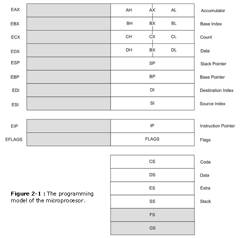
� ���� The programming model contains 8-, 16-, and 32-fleck registers. The 8-bit registers are AH, AL, BH, BL, CH, CL, DH, and DL and are referred to when an teaching is formed using these 2-letter of the alphabet designations. The 16-bit registers are AX, BX, CX, DX, SP, BP, DI, SI, IP, FLAGS, CS, DS, ES, SS, FS, and GS. The extended 32-scrap registers are EAX, EBX, ECX, EDX, ESP, EBP, EDI, ESI, EIP, and EFLAGS. These 32-bit extended registers, and 16-bit registers ES and GS are available only in the 80386 and in a higher place.
Some registers are full general-purpose or multipurpose registers, while some accept special purposes. The multipurpose registers include EAX, EBX, ECX, EDX, EBP, EDI, and ESI. These registers hold various data sizes (bytes, words, or doublewords) and are used for almost any purpose, as dictated by a program.
2.1.1.1. Multipurpose Registers
EAX (accumulator)
EAX is referenced as a 32-fleck register (EAX), equally a 16-bit register (AX), or as either of ii 8-bit registers (AH and AL). Note that if an 8- or sixteen-bit register is addressed, only that portion of the 32-bit register changes without affecting the remaining bits. The accumu�lator is used for instructions such as multiplication, partitioning, and some of the adjustment instructions. For these instructions, the accumulator has a special purpose, only is by and large considered to be a multipurpose register. In the 80386 and above, the EAX annals may also hold the start address of a location in the retentivity system.
EBX (base of operations index)
EBX is addressable as EBX, BX, BH, or BL. The BX register sometimes holds the beginning accost of a location in the retentiveness organization in all versions of the microprocessor. In the 80386 and higher up, EBX also can accost retentiveness data.
ECX (count)
ECX is a full general-purpose register that also holds the count for diverse instructions. In the 80386 and higher up, the ECX register as well can agree the starting time address of retention data. Instructions that use a count are the repeated cord instructions (REP/REPE/REPNE); and shift, rotate, and LOOP/LOOPD instructions. The shift and rotate instructions utilize CL equally the count, the repeated string instructions employ CX, and the LOOP/LOOPD instructions use either CX or ECX.
EDX (data)
EDX is a full general-purpose register that holds a role of the consequence from a multiplication or part of the dividend earlier a partitioning. In the 80386 and above, this register can likewise address retention information.
EBP (base arrow)
EBP points to a memory location in all versions of the micropro�cessor for memory data transfers. This register is addressed as either BP or EBP.
EDI (destination index)
EDI oft addresses string destination data for the cord instruc�tions. It also functions as either a 32-bit (EDI) or 16-chip (DI) general-purpose register.
ESI (source index)
ESI is used as either ESI or SI. The source alphabetize register often addresses source string data for the cord instructions. Like EDI, ESI also functions as a full general-purpose annals. Equally a xvi-bit register, it is addressed as SI; as a 32-bit register, information technology is addressed as ESI.
2.1.1.2. Special-purpose Registers.
The special-purpose registers include EIP, ESP, EFLAGS; and the segment registers CS, DS, ES, SS, FS, and GS.
EIP (didactics pointer)
EIP addresses the adjacent instruction in a department of memory defined as a code segment. This annals is IP (sixteen $.25) when the micropro�cessor operates in the real mode and EIP (32 bits) when the 80386 and above operate in the protected manner. Note that the 8086, 8088, and 80286 practise contain EIP, and merely the 80286 and above operate in the protected mode. The didactics pointer, which points to the side by side instruction in a program, is used past the microprocessor to find the next sequential didactics in a program located within the code segment. The pedagogy pointer can exist modified with a spring or a phone call instruction.
ESP (stack pointer)
ESP addresses an area of retentiveness called the stack. The stack memory stores data through this pointer. This register is referred to every bit SP if used as a xvi-hitting annals and ESP if referred to every bit a 32-bit annals.
EFLAGS
EFLAGS indicate the status of the microprocessor and command its operation. Figure 2-two shows the flag registers of all versions of the microprocessor. Note that the flags are upward-compatible from the 8086/8088 to the Pentium II microprocessor. The 8086-80286 contain a FLAG register (16 bits) and the 80386 and above contain an EFLAG annals (32-chip extended flag register).
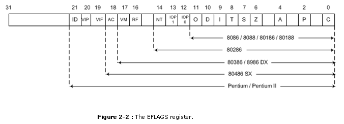
The rightmost five flag bits and the overflow flag change after many arithmetic and logic in�structions execute. The flags never alter for any information transfer or program control operation. Some of the flags are also used to control features found in the microprocessor. Following is a list of each flag flake, with a cursory description of their function.
C (carry)
Carry holds the carry later add-on or the borrow after subtraction. The carry flag also indicates error conditions, every bit dictated by some programs and procedures. This is especially true of the DOS func�tion calls.
P (parity)
Parity is a logic 0 for odd parity and a logic ane for even parity. Parity is a count of ones in a number expressed as fifty-fifty or odd.
If a number contains zero one bits, it has even parity. The parity flag finds little application in modernistic programming and was implemented in early Intel microprocessors for checking data in data communications environments. Today parity checking is often accomplished by the data communications equipment instead of the microprocessor.
A (auxiliary carry)
The auxiliary deport holds the behave (half-carry) after improver or the borrow after subtraction between $.25 positions iii and iv of the result. This highly specialized flag scrap is tested by the DAA and DAS instructions to accommodate the value of AL later a BCD improver or subtraction. Otherwise, the A flag bit is not used by the microprocessor or whatsoever other instructions.
Z (zero)
The aught flag shows that the event of an arithmetic or logic opera�tion is nil. If Z=one, the upshot is zero; if Z= 0, the issue is not zero.
S (sign)
The sign flag holds the arithmetic sign of the event afterward an arithmetics or logic pedagogy executes. If S= ane, the sign fleck (leftmost hit of a number) is set or negative; if Due south=0, the sign flake is cleared or positive.
T (trap)
The trap flag enables trapping through an on-scrap debugging feature. (A program is debugged to find an error or bug.) If the T flag is enabled (1), the microprocessor interrupts the flow of the program on weather condition as indicated by the debug registers and control registers. lf the T flag is a logic 0, the trapping (debugging) feature is disabled.
I (interrupt)
The interrupt flag controls the functioning of the INTR (interrupt request) input pin. If I = 1. the INTR pin is enabled: if I = 0, the INTR pin is disabled. The state of the I flag bit is controlled by the STI (set I flag) and CLI (clear I flag) instructions.
D (management)
The direction flag selects either the increment or decrement way for the Dl and/or SI registers during string instructions. If D=1, the registers are automatically decremented: if D=1, the registers are automatically incremented. The D flag is gear up with the STD (set direction) and cleared with the CLD (articulate direction) instructions.
0 (overflow)
Overflows occurs when signed numbers are added or subtracted. An overflow indicates that the result has exceeded the capacity of the automobile. For unsigned operations, the overflow flag is ignored.
IOPL (I/0 privilege level)
IOPL is used in protected way operation to select the privilege level for I/O devices. If the current privilege level is higher or more trusted than the IOPL, I/O executes without hindrance. If the IOPL is lower than the current privilege level, an interrupt occurs, causing execution to append. Note that an IOPL of 00 is the highest or most trusted: if IOPL is 11, � � it is the lowest or least trusted.
NT (nested chore)
The nested task flag indicates that the current task is nested within another task in protected mode functioning. This line is ready when the task is nested by software.
RF (resume)
The resume flag is used with debugging to control the resumption of execution later the next pedagogy.
VM (virtual mode)
The VM flag fleck selects virtual manner operation in a protected mode system. A virtual style system allows multiple DOS memory par�titions that are 1M byte in length to coexist in the memory arrangement. Essentially, this allows the arrangement program to execute multiple DOS programs.
Ac (alignment check)
The alignment check flag bit activates if a discussion or douhleword is addressed on a non-word or not-douhleword purlieus. Only the 80486SX microprocessor contains the alignment check hit that is primarily used by its companion numeric coprocessor, the 80487SX, for synchronization.
VIF (virtual interrupt flag)
The VIF is a copy of the interrupt flag scrap available to the Pentium-Pentium II microprocessors.
VIP (virtual interrupt pending)
VIP provides information most a virtual mode interrupt for the Pentium�Pentium II microprocessors. This is used in multitasking environments to provide the operating system with virtual interrupt flags and interrupt pending information.
ID (identification)
The ID flag indicates that the Pentium�Pentium II microprocessors support the CPUID instruction. The CPUID education provides the system with information nigh the Pentium microprocessor, such as its version number and manufacturer.
2.1.1.three. Segment Registers
Additional registers, called segment registers, generate memory addresses when combined with other registers in the microprocessor. There are either iv or vi segment registers in various versions of the microprocessor. A segment register functions differently in the real mode when compared to the protected manner operation of the microprocessor. Following is a list of each segment register, along with its function in the system:
CS (code)
The code segment is a section of memory that holds the lawmaking (programs and procedures) used by the microprocessor. The code segment register defines the starting address of the section of memory holding code. In real way operation, it defines the kickoff of a 64K-byte section of retentivity; in protected mode, it selects a descriptor that describes the starting accost and length of a section of memory holding lawmaking. The code segment is express to 64K bytes in the 8088-80286, and 4G bytes in the 80386 and above when these microprocessors operate in the protected style.
DS (data)
The data segment is a section of retention that contains virtually information used past a programme. Data are accessed in the data segment by an outset address or the contents of other registers that concur the beginning address. As with the code segment and other segments, the length is limited to 64K bytes in the 8086-80286, and 4G bytes in the 80386 and higher up.
ES (extra)
The extra segment is an boosted data segment that is used past some of the string instructions to concord destination data.
SS (stack)
The stack segment defines the area of memory used for the stack. The stack entry point is determined past the stack segment and stack arrow registers. The BP register too addresses information within the stack segment.
FS and GS
The FS and GS segments are supplemental segment registers bachelor in the 80386, 80486, Pentium. and Pentium Pro microprocessors to allow two additional memory segments for admission past programs.
2.2. Real Mode Retentivity Addressing
�������� The 80286 and above operate in either the existent or protected mode. Only the 8086 and 8088 op�erate exclusively in the existent mode. Real mode operation allows the microprocessor to address merely the first 1M byte of retentivity space-fifty-fifty if it is the Pentium 2 microprocessor. Note that the first ane M byte of retentiveness is called either the real memory or conventional memory organization. The DOS operating organization requires the microprocessor to operate in the real way. Real mode oper�ation allows application software written for the 8086/8088, which contain merely i M byte of memory, to office in the 80286 and above without irresolute the software. The upward com�patibility of software is partially responsible for the continuing success of the Intel family of mi�croprocessors. In all cases, each of these microprocessors begins operation in the real way past default whenever power is applied or the microprocessor is reset.
ii.2.1. Segments And Offsets
�������� A combination of a segment accost and an start accost, access a retention location in the real mode. All real mode retention addresses must consist of a segment accost plus an outset accost. The segment address, located within one of the segment registers, defines the starting time accost of any 64K-byte memory segment. The offset address selects whatever location within the 64K byte retentiveness segment. Segments in the real mode e'er take a length of 64K bytes. Effigy two-three shows how the segment plus offset addressing scheme selects a memory location. This illustra� tion shows a memory segment that begins at location i 0000H and ends at location one FFFEH 64K bytes in length. Information technology likewise shows how an starting time address, sometimes called a displacement, of F000H selects location ������������1F000H in the retentivity system. Note that the first or displacement is the altitude to a higher place the start of the segment, equally shown in Figure 2-3.
������ The segment register in Effigy 2-three contains a 1000H, nonetheless it addresses a starting segment at location 10000H. In the real mode, each segment register is internally appended with a 0H on its rightmost end. This forms a twenty-bit memory address, assuasive it to access the start of a segment. The microprocessor must generate a twenty-hitting retentivity address to access a location within the first ane M of memory. For case, when a segment register contains a 1200H, it addresses a 64K-byte memory segment get-go at location 12000H. Likewise, if a segment register contains a 1201H, it addresses a retention segment starting time at location 12010H. Because of the internally ap�pended 0H, real mode segments can begin simply at a 16-byte boundary in the memory system. This 16-byte boundary is often called a paragraph.
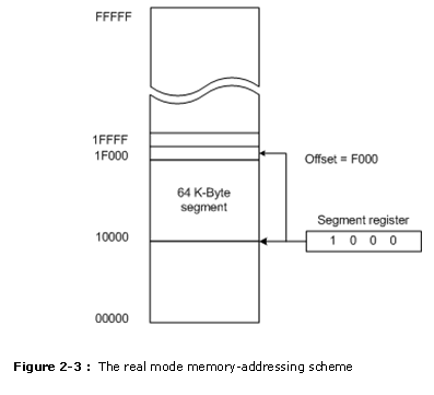
Because a real way segment of retention is 64K in length, one time the starting time address is known, the ending address is found by adding FFFFH.
The kickoff address, which is a part of the address, is added to the start of the segment to ad�wearing apparel a memory location within the memory segment. For example, if the segment address is 1000H and the offset address is 2000H, the microprocessor addresses memory location 12000H. The kickoff address is always added to the starting address of the segment to locate the data. The segment and offset address is sometimes written equally 1000:2000 for a segment address of 1000H with an start of 2000H.
In the 80286 (with special external circuitry), and the 80386 through the Pentium Two, an extra 64K minus 16 bytes of memory is addressable when the segment address is FFFFH and the HIMEM.SYS driver is installed in the system. This surface area of memory (0FFFF0H-10FFEFH) is re�ferred to as high memory.
Some addressing modes combine more than one register and an first value to form an offset accost. When this occurs, the sum of these values may exceed FFFFH. For example, the address accessed in a segment whose segment address is 4000H, and whose offset address is specified every bit the sum of F000H plus 3000H, volition access memory location 42000H instead of lo�cation 52000H. When the F000H and 3000H are added, they form a sixteen-bit (modulo 16) sum of 2000H used every bit the beginning address; not 12000H, the true sum. Note that the acquit of 1 (F000H + 3000H=12000H) is dropped for this addition to course the offset address of 2000H. This ways that the address is generated as 4000:2000 or 42000H.
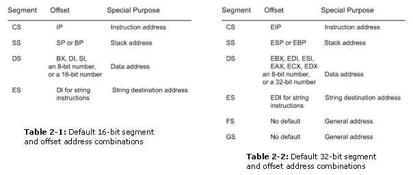
2.two.2. Default Segment and Get-go Registers
�������� The microprocessor has a prepare of rules that employ to segments whenever memory is addressed, These rules, which utilize in the existent and protected fashion, define the segment register and offset annals combination. For example, the code segment register is always used with the instruction pointer to address the next didactics in a program. This combination is CS:IP or CS:EIP, de�pending upon the microprocessor�s mode of functioning. The code segment register defines the showtime of the code segment and the teaching pointer locates the side by side education inside the code segment. This combination (CS:IP or CS:EIP) locates the next instruction executed by the mi�croprocessor.
Some other of the default combinations is the stack. Stack information are referenced through the stack segment at the memory location addressed by either the stack arrow (SP/ESP) or the base pointer (BP/EBP). These combinations are referred to equally SS:SP (SS:ESP) or SS:BP (SS:EBP). Note that in real mode, only the rightmost xvi $.25 of the extended annals accost a location inside the memory segment. In the 80386�Pentium II, never place a number larger than FFFFH into an kickoff register if the microprocessor is operated in the real style. This causes the system to halt and point an addressing mistake.
Other defaults are shown in Tabular array 2-one for addressing memory using whatever Intel micropro�cessor with 16-scrap registers. Table two-2 shows the defaults causeless in the 80386 and above when using 32-fleck registers. Annotation that the 80386 and above have a far greater selection of segment offset address combinations than practise the 8086 through the 80286 microprocessors.
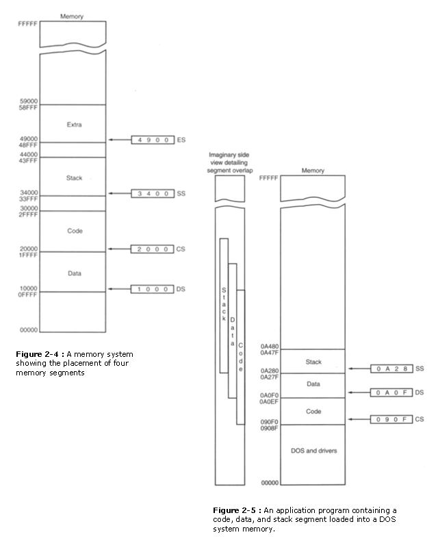
The 8086-80286 microprocessors allow four retentiveness segments and the 80386 and above let six retentiveness segments. Figure 2-iv shows a system that contains four memory segments. Note that a retentiveness segment can touch or fifty-fifty overlap if 64K bytes of memory are not required for a segment. Call back of segments every bit windows that tin can be moved over whatever area of retentivity to air-conditioning�assessment data or code. As well notation that a plan tin can have more than 4 or six segments, only can only access 4 or six segments at a time.
Suppose that an application program requires 1000H bytes of memory for its code, 190H bytes of memory for its data, and 200H bytes of retentiveness for its stack. This application does not require an actress segment. When this program is placed in the memory system past DOS, it is loaded in the TPA at the commencement available area of memory above the drivers and other TPA pro�grams. This area is indicated by a free-pointer that is maintained by DOS. Program loading is handled automatically by the programme loader located within DOS. Figure 2-5 shows how this application is stored in the memory system. The segments prove an overlap because the amount of information in them does not require 64K bytes of memory. The side view of the segments clearly shows the overlap. Information technology also shows how segments can exist moved over any area of retentiveness past changing the segment starting address. Fortunately, the DOS program loader calculates and as�signs segment starting addresses.
2.2.3. Segment and Offset Addressing Scheme Allows Relocation
�������� The segment and offset addressing scheme seems disproportionately complicated. It is complicated, but information technology too affords an advantage to the arrangement. This complicated scheme of segment plus offset ad�dressing allows programs to exist relocated in the retention organisation. Information technology as well allows programs written to role in the real style to operate in a protected mode organisation. A relocatable pro�gram is i that tin be placed into any surface area of retention and executed without alter. Relocat�able data are information that tin can be placed in whatever area of memory and used without whatsoever change to the program. The segment and outset addressing scheme allows both programs and data to be relo�cated without changing a matter in a program or information. This is ideal for employ in a general-purpose computer system in which non all machines contain the same retentivity areas. The personal estimator retention structure is different from machine to machine, requiring relocatable soft�ware and data.
Considering memory is addressed within a segment past an offset address, the memory segment can exist moved to any identify in the memory organization without changing any of the offset addresses. This is accomplished by moving the entire plan, as a block, to a new area then changing simply the contents of the segment registers. If an instruction is iv bytes above the start of the seg�ment, its beginning accost is 4. If the unabridged program is moved to a new area of memory, this offset address of 4 still points to iv bytes above the start of the segment. Merely the contents of the seg�ment register must be changed to address the program in the new expanse of retention. Without this feature, a plan would have to be extensively rewritten or contradistinct before it is moved. This would crave additional time or many versions of a program for the many different configura�tions of computer systems.
2.three. Introduction to Protected Manner Retentiveness Addressing
�������� Protected style memory addressing (80286 and above) allows access to information and programs lo�cated above the first 1M byte of memory, every bit well as inside the outset 1M byte of memory. Ad�dressing this extended section of the memory system requires a modify to the segment plus an offset addressing scheme used with real fashion memory addressing. When data and programs are addressed in extended memory, the showtime accost is still used to access information located inside the memory segment. One difference is that the segment address, is no longer present in the protected fashion. In place of the segment ad�dress, the segment annals contains a selector that selects a descriptor from a descriptor tabular array. The descriptor describes the retentiveness segment�s location, length, and access rights. Because the segment register and offset address withal access memory, protected mode instructions are iden�tical to real way instructions. In fact, most programs written to part in the existent manner will office without alter in the protected mode. The deviation between modes is in the fashion that the segment register is interpreted by the microprocessor to access the retentiveness segment. An�other difference, in the 80386 and above, is that the start address can be a 32-bit number instead of a 16-scrap number in the protected fashion. A 32-bit get-go address allows the microprocessor to access data within a segment that tin can be up to 4G bytes in length.
2.3.ane. ����Selectors And Descriptors
�������� The selector, located in the segment register, selects one of 8192 descriptors from one of two ta�bles of descriptors. The descriptor describes the location, length, and access rights of the seg�ment of memory. Indirectly, the segment annals all the same selects a memory segment, but not direct as in the real mode. For case, in the real fashion, if CS = 0008H, the code segment begins at lo�cation 00080H. In the protected mode, this segment number can address any retentivity location in the unabridged arrangement for the code segment.
�� There are ii descriptor tables used with the segment registers: 1 contains global de�scriptors and the other contains local descriptors. The global descriptors contain segment defini�tions that apply to all programs, while the local descriptors are unremarkably unique to an application. You might call a global descriptor a organisation descriptor and call a local descriptor an application descriptor. Each descriptor tabular array contains 8192 descriptors, so a total of 16,384 total descriptors are bachelor to an application at any fourth dimension. Considering the descriptor describes a retentiveness segment, this allows up to 16,384 memory segments to be described for each application.
Figure 2-6 shows the format of a descriptor for the 80286 through the Pentium II. Note that each descriptor is 8 bytes in length, then the global and local descriptor tables are each a max�imum of 64K bytes in length. Descriptors for the 80286 and the 80386 through the Pentium Ii differ slightly, but the 80286 descriptor is upward-compatible.
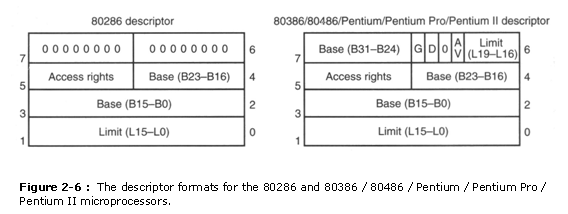
The base of operations address portion of the descriptor indicates the starting location of the memory segment. For the 80286 microprocessor, the base accost is a 24-fleck accost, so segments begin at whatever location in its 16M bytes of retention. Annotation that the paragraph boundary limitation is re�moved in these microprocessors when operated in the protected mode. The 80386 and above use a 32-bit base address that allows segments to begin at whatever location in its 4G bytes of retentivity. Notice how the 80286 descriptor�s base address is upwards-compatible to the 80386 through the Pentium II descriptor because its most-pregnant 16 bits are 0000H. �
The segment limit contains the last first address found in a segment. For instance, if a segment begins at memory location F00000H and ends at location F000FFH, the base address is F00000H and the limit is FFH. For the 80286 microprocessor, the base of operations address is F00000H and the limit is OOFFH. For the 80386 and above, the base address is 00F00000H and the limit is 000FFH. Notice the limit the 80286 has a 16-fleck limit and the 80386 through the Pentium 2 have a 20-bit limit. The 80286 accesses memory segments that are betwixt ane and 64K bytes in length. The 80386 and higher up admission memory segments that are between 1 and ane M byte, or 4K and 4G bytes in length.
At that place is another characteristic found in the 80386 through the Pentium II descriptor that is non found in the 80286 descriptor: the G bit, or granularity bit. If Thousand = 0, the limit specifies a seg�ment limit of 00000H to FFFFFH. If Thousand = one, the value of the limit is multiplied by 4K bytes (ap�pended with XXXH). The limit is then 00000XXXH to FFFFFXXXH, if G = 1. This allows a segment length of 4K to 4G bytes in steps of 4K bytes. The reason that the segment length is 64K bytes in the 80286 is that the offset address is e'er 16 bits because of its 16-chip internal archi�tecture. The 80386 and above use a 32-bit architecture that allows an offset address, in the pro�tected mode operation, of the 32 bits. This 32-scrap commencement address allows segment lengths of 4G bytes and the sixteen-bit outset accost allows segment lengths of 64K bytes. Operating systems op�erate in a xvi or 32-bit environs. For example, DOS uses a xvi-bit environment, while most Windows applications use a 32-flake environment.
The AV bit, in the 80386 and above descriptor, is used by some operating systems to indi�cate that the segment is available (AV = 1) or non available (AV = 0). The D bit indicates how the 80386 through the Pentium 2 instructions access register and memory data in the protected or real mode. If D=0, the instructions are 16-flake instructions, uniform with the 8086�80286 mi�croprocessors. This means that the instructions use xvi-bit offset addresses and sixteen-bit registers by default. This manner is often called the 16-bit instruction fashion. If D=i, the instructions are 32-bit instructions. By default, the 32-bit education mode assumes that all offset addresses and all registers are 32 bits. Note that the default for register size and offset address size can be overridden in both the 16- and 32-bit pedagogy modes. Both the MSDOS and PCDOS oper�ating systems require that the instructions are ever used in the 16-fleck instruction mode. Win�dows 3.1 likewise requires that the 16-scrap educational activity mode is selected. Note that the 32-scrap instruction way is attainable simply in a protected-mode system such as Windows NT, Windows 95, Windows 98, or OS/2.
�The access rights byte in Effigy 2-7 controls access to the protected fashion memory segment. This byte describes how the segment functions in the system. The access rights byte al�lows consummate command over the segment. If the segment is a data segment, the management of growth is specified. If the segment grows beyond its limit, the microprocessor�southward program is interrupted, indicating a full general protection mistake. You tin can fifty-fifty specify whether a data segment can be written or is write-protected. The code segment is also controlled in a similar way and can accept reading inhibited to protect software.
Descriptors are called from the descriptor tabular array by the segment annals. Figure ii-8 shows how the segment register functions in the protected manner organization. The segment register contains a 13-bit selector field, a tabular array selector flake, and a requested privilege level field. The 13-chip selector chooses one of the 8192 descriptors from the descriptor table. The TI fleck selects ei�ther the global descriptor table (TI = 0) or the local descriptor table (TI = 1). The requested privilege level (RPL) requests the admission privilege level of a retentiveness segment. The highest privilege level is 00 and the lowest is 11. If the requested privilege level matches or is higher in priority than the privilege level prepare by the access rights byte, admission is granted. For instance, if the requested privilege level is x and the access rights byte sets the segment privilege level at 11, access is cvranted because 10 is higher in priority than privilege level 11. Privilege levels are used in multiuser environments. If the privilege level is violated, the system normally indicates a 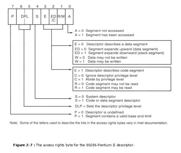 privilege violation.
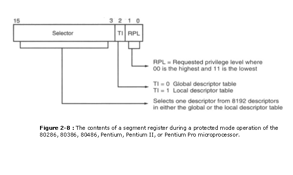
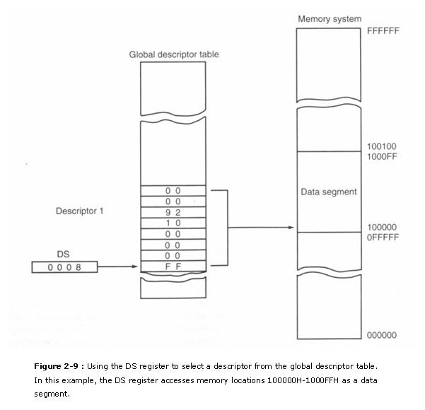
Figure 2-9 shows how the segment annals, containing a selector, chooses a descriptor from the global descriptor table. The entry in the global descriptor table selects a segment in the memory system. In this illustration, DS contains 0008H, which accesses the descriptor number i from the global descriptor table past using a requested privilege level of 00. Descriptor number i contains a descriptor that defines the base of operations address as 00100000H with a segment limit of 000FFH. This means that a value of 0008H loaded into DS causes the microprocessor to use retention locations 00100000H�001000FFH for the data segment with this instance descriptor table. Notation that de�scriptor null is called the zero descriptor and may non be used for accessing retention.
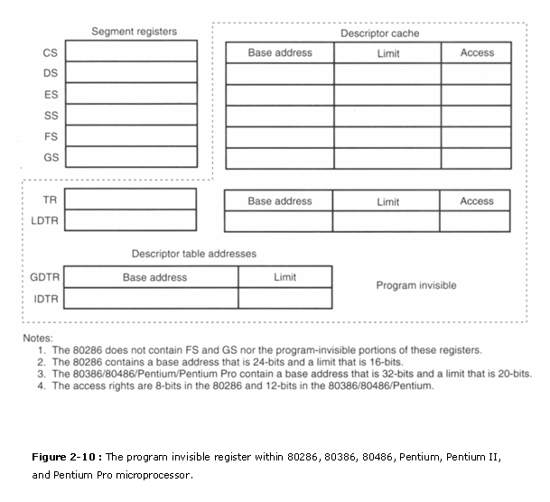
ii.3.two. Program-Invisible Registers
�������� The global and local descriptor tables are institute in the memory system. In society to admission and specify the address of these tables, the 80286, 80386, 80486, Pentium, Pentium Pro, and Pentium Ii incorporate programme-invisible registers. The program-invisible registers are not straight addressed past software and then they are given this proper noun (although some of these registers are accessed by the organisation software). Figure two-10 illustrates the program-invisible registers as they appear in the 80286 through the Pentium II. These registers control the microprocessor when operated in the protected fashion.
�� Each of the segment registers contains a plan-invisible portion used in the protected style. The programme-invisible portion of these registers is often called enshroud memory because a cache is any memory that stores information. This enshroud is not to be confused with the normal level ane or level 2 caches establish with the microprocessor. The program-invisible portion of the seg�ment register is loaded with the base accost, limit, and access rights each time the number in the segment register is inverse. When a new segment number is placed in a segment register, the mi�croprocessor accesses a descriptor table and loads the descriptor into the program-invisible enshroud portion of the segment register. It is held there and used to access the retentiveness segment until the segment number is over again changed. This allows the microprocessor to repeatedly admission a memory segment without referring to the descriptor table for each access (hence the term enshroud).
The GDTR (global descriptor table register) and IDTR (interrupt descriptor table reg�ister) comprise the base address of the descriptor table and its limit. The limit of each descriptor table is sixteen bits considering the maximum tabular array length is 64K bytes. When the protected mode oper�ation is desired, the address of the global descriptor table and its limit are loaded into the GDTR.
Earlier using the protected manner, the interrupt descriptor table and the IDTR must also exist ini�tialized. More detail is provided on protected manner performance afterwards in the text. At this point, the programming and boosted description of these registers are impossible.
The location of the local descriptor table is selected from the global descriptor table. One of the global descriptors is ready up to address the local descriptor table. To access the local descriptor table, the LDTR (local descriptor table annals) is loaded with a selector, simply as a segment reg�ister is loaded with a selector. This selector accesses the global descriptor tabular array and loads the base accost, limit, and access rights of the local descriptor table into the cache portion of the LDTR.
The TR (task annals) holds a selector, which accesses a descriptor that defines a task. A task is most often a procedure or application program. The descriptor for the process or applica�tion plan is stored in the global descriptor table, then access can be controlled through the privi�lege levels. The job register allows a context or task switch in about 17 � s. Task switching allows the microprocessor to switch between tasks in a fairly short amount of time. The task switch allows multitasking systems to switch from one task to another in a elementary and orderly style.
ii.4. Retention Paging
����������� The memory paging mechanism located within the 80386 and to a higher place allows any physical memory location to exist assigned to any linear address. The linear accost is defined as the accost generated by a program. With the retentiveness paging unit of measurement, the linear address is invisibly translated into whatever physical address, which allows an application written to function at a specific address to be re�located through the paging mechanism. It too allows retentiveness to be placed into areas where no retentiveness exists. An case is the upper memory blocks provided past EMM386.EXE.
The EMM386.EXE program reassigns extended memory, in 4K blocks, to the system retention between the video BIOS and the system BIOS ROMS for upper retentiveness blocks. With�out the paging mechanism, the use of this expanse of retentiveness is incommunicable.
2.4.one. Paging Registers
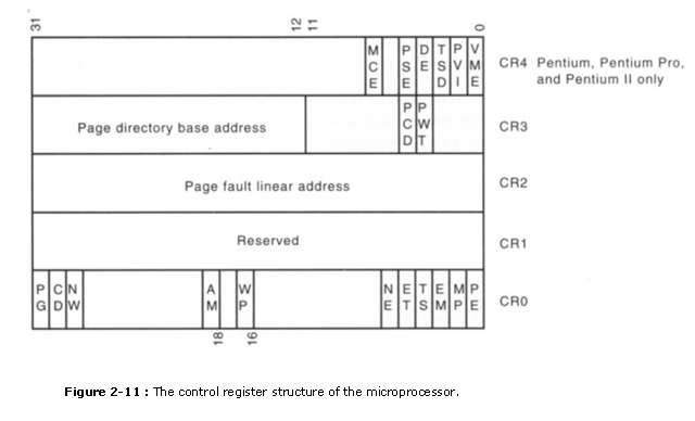
�������� The paging unit of measurement is controlled by the contents of the microprocessor�south control registers. See Fig�ure ii-xi for the contents of control registers CR0 through CR3. Note that these registers are just bachelor to the 80386 through the Pentium microprocessors. Get-go with the Pentium, an addi�tional control register labeled CR4 controls extensions to the basic architecture provided in the Pen�tium and above microprocessors. One of these features is a 4M-byte page that is enabled by setting bit position 4, or CR4.
�� The registers important to the paging unit are CR0 and CR3. The leftmost bit (PG) position of CR0 selects paging when placed at a logic 1 level. If the PG chip is cleared (0), the linear ad�dress generated by the program becomes the physical address used to access memory. If the PG bit is ready (1), the linear address is converted to a physical address through the paging machinery. The paging mechanism functions in both the real and protected modes.
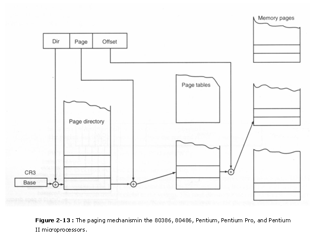
�� CR3 contains the page directory base address, and the PCD and PWT $.25. The PCD and PWT $.25 control the performance of the PCD and PWT pins on the microprocessor. If PCD is prepare (ane), the PCD pin becomes a logic one during bus cycles that are not pages. This allows the external hardware to control the level 2 enshroud retentiveness. (Notation that the level two cache memory is an external loftier-speed retentiveness that functions as a buffer between the microprocessor and the main DRAM memory organization.) The PWT bit as well appears on the PWT pin, during double-decker cycles that are non pages, to control the write-through enshroud in the arrangement. The folio directory base of operations accost locates the page directory for the folio translation unit of measurement. Note that this address locates the page directory at whatever 4K boundary in the memory system considering it is appended internally with a 000H. The folio directory contains 1024 directory entries of 4 bytes each. Each page directory entry addresses a folio table that contains 1024 entries.
The linear accost, equally information technology is generated past the software, is broken into three sections that are used to access the page directory entry, folio tabular array entry, and page offset accost. Figure 2-12 shows the linear address and its makeup for paging. Notice how the leftmost ten bits address an entry in the page directory. For linear address 00000000H�003FFFFFH, the start entry of the page directory is accessed. Each page directory entry represents or repages a 4M-byte section of the memory system. The contents of the page directory select a page table that is indexed by the adjacent x $.25 of the linear address (chip positions 12-21). This means that address 00000000H� 00000FFFH selects page directory entry 0 and page table entry 0. Discover this is a 4K-byte ad�dress range. The offset office of the linear address (bit positions 0-11) next selects a byte in the 4K-byte retention folio. In Effigy 2-12, if the page tabular array 0 entry contains accost 00100000H, then the physical address is 00100000H-00100FFFH for linear address 00000000H-00000FFFH. This means that when the program accesses a location between 00000000H and 00000FFFH, the microprocessor physically addresses location 00100000H�00100FFFH.
Because the act of repaging a 4K-byte section of memory requires admission to the page di�rectory and a page table, which are both located in retentivity, Intel has incorporated a cache called the TLB (translation look-aside buffer). In the 80486 microprocessor, the cache holds the 32 most recent page translation addresses. This means that the last 32 folio table translations are stored in the TLB, so if the same area of memory is accessed, the address is already nowadays in the TLB, and access to the page directory and page tables is not required. This speeds program exe�cution. If a translation is not in the TLB, the folio directory and page table must be accessed, which requires additional execution time. The Pentium, Pentium Pro, and Pentium II contain dissever 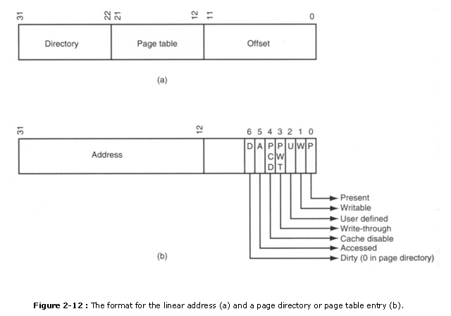 TLBs for each of their pedagogy and data caches.
two.4.two. The Page Directory and Page Table
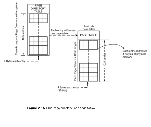
�������� Figure 2-xiii shows the page directory, a few page tables, and some retentivity pages. There is just ane folio directory in the system. The page directory contains 1024 doubleword addresses that locate up to 1024 page tables. The folio directory and each page table are 4K bytes in length. If the unabridged 4G byte of memory is paged, the system must allocate 4K bytes of retentiveness for the page directory, and 4K times 1024 or 4M bytes for the 1024 page tables. This represents a con�siderable investment in retention resources.
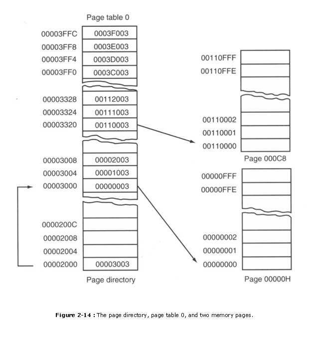
The DOS system and EMM386.EXE employ page tables to redefine the surface area of retentiveness be�tween locations C8000H�EFFFFH every bit upper retentivity blocks. Information technology does this by repaging extended retentivity to back-fill this part of the conventional memory organization to permit DOS admission to addi�tional memory. Suppose that the EMM386.EXE program allows access to 16M bytes of ex�tended and conventional memory through paging and locations C8000H�EFFFFH must be repaged to locations 110000�138000H, with all other areas of retention paged to their normal lo�cations. Such a scheme is depicted in Figure 2-14.
Hither, the page directory contains four entries. Think that each entry in the page directory corresponds to 4M bytes of physical memory. The system likewise contains four page tables with 1024 entries each. Recall that each entry in the folio table repages 4K bytes of concrete retentivity. This scheme requires a total of 16K of memory for the four page tables and 16 bytes of memory for the page directory.
As with DOS, the Windows plan also repages the retention organization. At present, Windows version 3.11 supports paging for just l6M bytes of memory because of the amount of retentivity re�quired to shop the page tables. On the Pentium and Pentium Pro microprocessors, pages can be ei�ther 4K bytes in length or 4M bytes in length. Although no software currently supports the 4M-byte pages, as the Pentium II and more advanced versions pervade the personal computer, operating sys�tems of the future volition undoubtedly begin to back up 4M-byte retention pages.


What Is The Memory Buffer Register Size Of The Pentium Processor,
Source: https://www.byclb.com/TR/Tutorials/microprocessors/ch2_1.htm
Posted by: rossparloo.blogspot.com
0 Response to "What Is The Memory Buffer Register Size Of The Pentium Processor"
Post a Comment